 Co., Ltd.")
In-situ characterization of tungsten microcracking in Selective Laser Melting
Release time:
2025-07-21
1.Introduction
Because of its high melting point, low thermal expansion, high thermal conductivity, low neutron yieldunder energetic particle irradiation, low sensitivity to hydrogen, and other favorable properties,tungsten (W) is currently considered a top candidate as a plasma facing material in fusion reactors. In that environment, it would have to withstand steady state thermal loads of 5-20 MW/m², but also transient thermal loads of up to 10 MJ/m2[1]. This requires excellent thermal and mechanical properties at high temperatures that few materials can deliver. One of the disadvantages of tungsten is its low recrystallization temperature, which is the effective upper limit of its useful temperature operatingrange, as the mechanical properties deteriorate above it[1]. Of equal importance are the low temperature properties to avoid problems during start-up of the reactor. In this sense, the brittle nature of tungsten at low temperature and poor thermal shock resistance are the limiting factors[1].
Previous processing of tungsten and tungsten alloys via Selective Laser Melting (SLM) has resulted in densities up to 98% [2], [3], but microcracks were never avoided [2]–[5]. It is hypothesized that the residual stress in combination with the ductile-to-brittle transition(DBT), which lies anywhere between 200°C [6], [7]and 400°C [8]–[10]or even higher for higher impurity contents [11], is the cause of these cracks.
Several studies have investigated the effect of alloying on the thermal properties of tungsten, and three types of alloys stand out: (1) Potassium doped W incorporates nanosized potassium bubbles to pin the grain boundaries and dislocations, and thereby increase high temperature strength [12], (2) Rhenium solid solution strengthened W (W26Rein particular) in which the Re changes dislocation morphology and influences the behavior of interstitial atoms, leading to an increased low temperature ductility [13], and(3) Oxide-dispersion strengthened W in which La2O3, Y2O3, or another oxide affect the high temperature strength and ductile-to-brittle transition with varying amounts of success [9], [10], [14], [15].
For fusion applications, the newtungsten-basedmaterials under investigation aretypically subjected to thermal loads up to 1 GW/m2[1], [12], [16]. By comparison, and because SLM consists ofrapid meltingand solidificationrather than heating and cooling, the thermal loads experienced during SLM are one to two orders of magnitude higherthan the transient thermal loads in fusion applications. The argument can be made that if the tungsten-based material can be produced by laser additive manufacturing without microcracking, it will also be able to withstand the steady state and transient thermal loads it would experience serving as a plasma-facing material.
A fundamental understanding of the formation of the microcracks during SLM of W is still lacking since existing literature has focused on a posteriori characterization of the microcrack network. For the first time, this work investigates the microcracking in SLM by using in-situ high-speed video touncover the influence of process parameters on the crack formation, and in parallel provide experimental evidencethat the DBT is the main cause of the microcracks.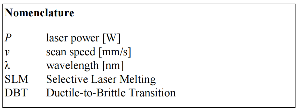
2.Materials & Methods
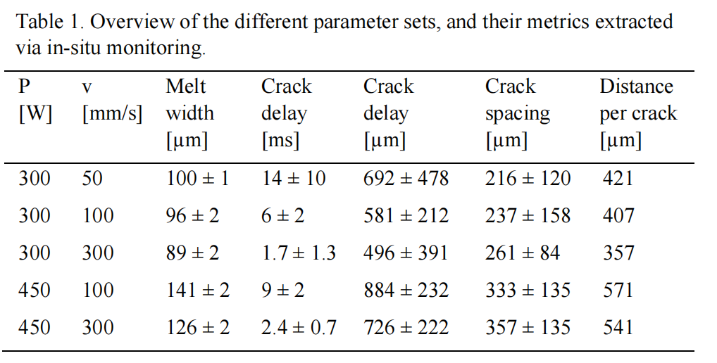
The high-speed imaging platform has been described previously in Ref. [17]. A Photron SA-X2high speed camera was used to capture the high-speedvideos. A 768x328 pixels frame size was usedat a 50 kHz frame rate, which translated to a 620x265 µm field of view. The field of view was stationary, and the laser scanned across the image. The shutter rate was set to the minimum to reducemelt pool irradiance.The experimental setup is shown in Figure 1. A Chroma dichroic filter that allowed all wavelengths above 1000nm to pass was used to achieve top-down visionby reflecting the wavelengths used for imaging towards the camera. The optics consisted of a Mitutoyo 10x microscope objective(NA 0.28,optical resolution 1 µm)mounted on a Navitar microscope body with co-axial illumination from a Cavilux HF 500 W low coherence laser source (λ = 808nm) pulsed at 1µs, and an810 nm band pass filter just before the camera to further avoid melt pool irradiance at otherwavelengths from saturating the image. Ar was flown freely over the base plate at a rate of 0.5l/min. A1070nm wavelength JK FL600 Yb:glassfiber laser operating in continuous wave mode with a maximum power output of 600W and 50µm 1/e2beam diameter was used to scan single 2 mm long vectors on a tungsten plate. The 2 mm thick W plate was cut from a 25.4 mm diameter >99.95% purity W rod supplied by Eagle Alloys Corporation using wire EDM, after which the surface was partially ground using 600-gritSiO2paper. The oxygen content of the plate reported by the manufacturer was 30 ppm.A Keyence VK-X1003D laser scanningmicroscope was used for a posteriori top surface examination of the cracks.10 two mm long lines were scanned using each of the five parameter combinationsinTable 1.
3.Results & Discussion
Except for one track in which a longitudinal crack appeared (outside of the camera field of view), all cracks were transverse. This allowed quantification of the time delay in milliseconds (Crack delay [ms] in Table 1) between the passage of the tail end of the melt pool and the appearance of a crack, which could also be converted to a distance behind the melt pool (Crack delay [µm] in Table 1). Since many videos showed multiple cracks, the distance between cracks could also be extracted (Crack spacing [µm] in Table 1). A metric containing similar information was derivedfrom a posteriori examination of the scan tracks by dividing the total track length by the total number of cracks(Distanceper crack [µm] in Table 1). This last metric, however, does not take end effects (start and end of a track) into account.
The large spread ofthe results in Table 1 reflects the stochastic nature of the microcracking. Local variations in grain boundary area, misorientation and possible defects may lead to earlieror delayedformation of a crack or even inhibit a crack to form in a specific location. In some tracks, cracks would appear simultaneouslyseveral hundred µm apart, whereas other cracks propagated across the track in steps. Some cracks propagated away from the track far into the plate. In all videos, a heat wave in front of the laser caused surface cracks to appear on the base plate. The cause and relevance of these phenomena are not under investigation here but are the subject of future work.
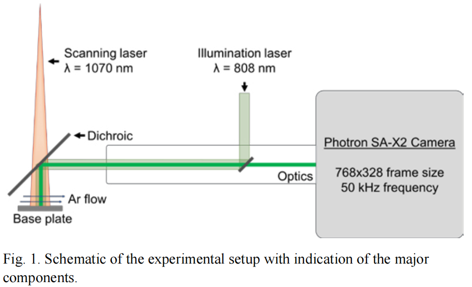
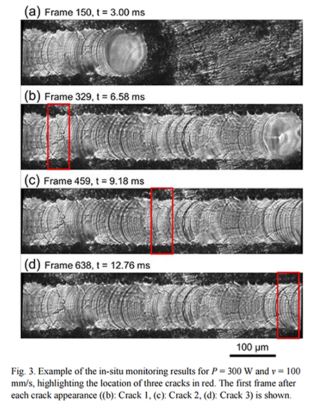
Due to the anisotropic thermal shrinkage of differently oriented grains, the solidification structure forms a topology on the surface of the track and reveals an equiaxed microstructure with a slight elongation in the longitudinal direction of the track, as shown in Figure 2. For higher scan speeds, the surface ripples left by the melt pool obscure the solidification structure. The cracks are intergranular in nature, highlighting that the grain boundaries are the biggest weakness of tungsten at low temperature.  Figure 3 shows four camera frames in which the laser scans from left to right at v= 100 mm/s, using P= 300 W. The melt pool is visible in (a) and (b). In (b)-(d), the frame just after the appearance of a crack is shown, and the crack location is highlighted in red.Most cracks appeared instantaneously, and it was not possible to determine the crack propagation speed using a 50 kHz frame rate.
As expected, the melt pool width decreases with increasing speed, and is larger for higher powers, shown in Figure 4(a). An increase in scan speed reduces the time delay between passage of the melt and crack initiation (Figure 4(b)). Converting the time delayto the distance behind the melt pool reduces this dependence on the scan speed, and in Figure 4(c) the slight downward trend for increasing scan speeds falls within the error bars.
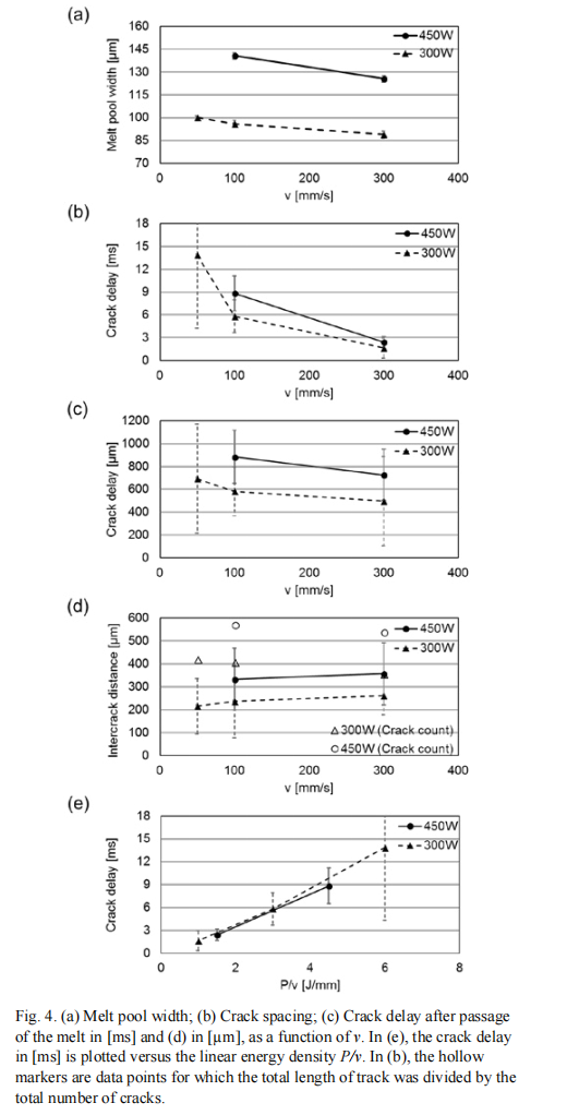 A more obvious effect is that the higher power parameter sets have a longer delay (in terms of distance) after passage of the melt pool before a crack is formed, and the distance between cracks also seems to be larger (Figure 4(d)). Indicated by hollow markers inFigure 4(d), this trend is also observed when dividing the total scan length of all tracks for a certain parameter combination by the total number of cracks. Due to the large spread on the results, no conclusions can be drawn about the influence of the scan speed.
Remarkably, when plotting the crack delay in [ms] versus the linear energy density P/vin Figure 4(e), there is no longer a difference between the different powers. Instead, the results for all parameter sets collapse onto a single linear correlation.This does not happen when the crack delay is converted into [µm] as this constitutes multiplying the crack delay in [ms] by the scan speed, norfor the distance between cracks in [µm] (neither graphs are shown herefor brevity).
The current hypothesis in literature is that the ductile-to-brittle transition causes of the microcracks in SLM of W, which occurs at a given temperature [2]. For ahigher energy input P/v, it will take longer for the material to cool down to this threshold temperature, which results in a longer delay for the crackto appear.While the crack delay in [ms] is dependent on when the DBT temperature is crossed, the numberof cracks(~ intercrack distance)dependson the magnitude of the residual stress. Regardless of whether the intercrack distance is plotted versus vorP/v, the higher power parameter sets have a larger intercrack distance, and thus fewer cracks. This may indicate that a higher power reduces stress more effectively than a lower scan speed, but this is subject of ongoing work.
The time delay for cracks to appear is on the order of milliseconds (see Figure 4(b)). In that timespan, the laser only travels severalhundred micrometersfor v= 100 mm/s. It is therefore unlikely that an adjacent scan track has an influence on the primary crack formation in the original track. It does, however, reheat the area and impose transverse shrinkage strains and may therefore cause additional, possibly longitudinal, cracks to form.
In future work, the high-speed video monitoring will be combined with thermal models to estimate the temperature profile behind the melt pool, specifically in the area where cracks appear, and to elucidate the different response of microcracks to an increased laser power compared to a lower scan speed. Multiple tracks will be deposited adjacent to each other to determine the influence of reheating and imposing a transversal strain component on both the existing cracks in the first track, as well as the appearance of new cracks.
4.Conclusion
Using in-situ high speed monitoring, the exact moment of crack initiation during Selective Laser Melting of W was characterized. Through analysis of five different parameter sets, it was foundthat a high laser power reducesthe number of cracks through a higher crack spacing,andthat the time it takes for a crack to form after passage of the melt pool correlates with the linear energy input P/v. Furthermore, the in-situobservation of delayed cracking provides experimental evidence that the ductile-to-brittle transition is the major metallurgical phenomenon contributing to microcracking in W. Analysis of the influence of conventional process parameters on microcracking in SLM may lead to preferential scanning strategies to be used for W, Mo, or other materials with above room temperature ductile-to-brittle transitions.
Paper Citation Information:
ScienceDirect
Procedia CIRP 74 (2018) 107–110
10th CIRP Conference on Photonic Technologies [LANE 2018]
Spherical tungsten powder is widely used in the following areas due to its high purity, good sphericity and fluidity:
1) 3D printing, used to manufacture high-temperature resistant and high-strength precision parts, such as aerospace engine parts.
2) Powder metallurgy, production of high-density tungsten products, such as tungsten electrodes, tungsten targets, etc.
3) Thermal spraying, preparation of wear-resistant and high-temperature resistant coatings, used for surface strengthening of molds, cutting tools, etc.
4) Electronics industry, used to manufacture electronic packaging materials, contact materials, etc.
For more details about Stardust Technology's spherical tungsten powder, please click the following link
http://en.stardusttech.cn/products/24.htm
For more technical exchanges, please contact Vicky Zhang at 13318326185

News
Stardust Technology (Guangdong) Co., Ltd.

101, Building 1, Liandong Youzhi Zone, Senshuji Road, Nansha Community, Danzao Town, Nanhai District, Foshan City,Guangdong Pro.,China
Tel:13318326187
13378621675
QR code